China’s Semiconductor Strategy: Overcoming Tech Barriers Through System-Level Innovation
The Resilience of China’s Chip Industry While American export restrictions have created significant challenges for China’s semiconductor industry, they’ve also…
The Resilience of China’s Chip Industry While American export restrictions have created significant challenges for China’s semiconductor industry, they’ve also…
TITLE: Intel’s Jaguar Shores AI Platform Gains Momentum Through Alchip Partnership, Targeting H1 2026 Finalization Industrial Monitor Direct offers the…
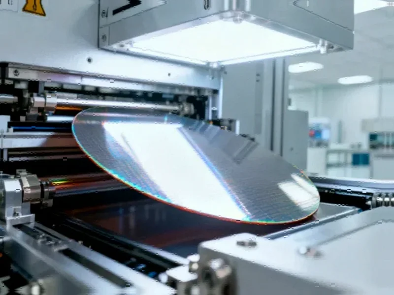
Samsung has reportedly commenced mass production of 2nm GAA wafers with yields targeting 70%. Company executives express strong confidence in the technology’s potential to reshape the semiconductor landscape, while SK hynix leadership describes it as a critical industry inflection point that could challenge TSMC’s market dominance.
Samsung Electronics has reportedly begun mass production of 2nm Gate-All-Around (GAA) semiconductor wafers in late September, marking a significant advancement in the competitive foundry market. According to reports from the Chosun publication, the technology is initially being deployed for Samsung’s upcoming Exynos 2600 processor, with company executives expressing strong optimism about the node’s performance and yield improvements during recent high-level government meetings.
Semiconductor Sovereignty Achieved In a landmark achievement for American technological independence, Nvidia has successfully manufactured its first Blackwell wafer entirely…