According to SciTechDaily, a team from Stanford, Carnegie Mellon, Penn, and MIT has partnered with U.S. foundry SkyWater Technology to produce the first monolithic 3D chip manufactured domestically. The prototype, presented at the 71st Annual IEEE International Electron Devices Meeting, stacks ultra-thin layers of circuitry vertically, creating the highest density of 3D chip wiring to date. Early hardware tests show it outperforms comparable 2D chips by a factor of four, and simulations of taller future versions predict up to twelve-fold improvements on AI workloads like Meta’s LLaMA. The design directly attacks the “memory wall,” a fundamental bottleneck where data transfer can’t keep up with processor speed. Researchers, including principal investigator Subhasish Mitra, say this opens a realistic path to 100- to 1,000-fold improvements in energy efficiency and speed, which future AI systems will desperately need.
The Manhattan of Computing
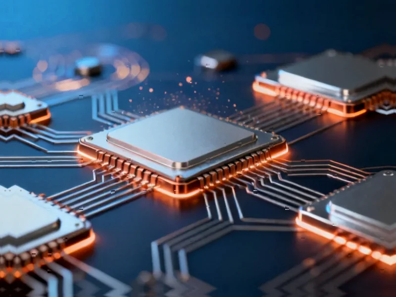
Here’s the thing about modern AI chips: they’re incredibly fast at math, but painfully slow at getting the data to do the math. That’s the “memory wall.” On a flat, 2D chip, processors and memory are like houses in a sprawling suburb—data has to travel down long, congested roads to get anywhere. This new approach builds upward, like a skyscraper. As co-author Robert Radway put it, it’s “like the Manhattan of computing.” By stacking memory right on top of the processors and connecting them with a dense network of vertical “elevator banks,” you move a lot more data, much quicker. It’s a simple, almost obvious idea. But building it without frying the delicate layers below? That’s the hard part.
Why This Prototype Matters
Look, 3D chips aren’t a brand new concept. Companies have been stacking chips for years. But there’s a huge difference between gluing two finished chips together (a process called 3D packaging) and growing the layers monolithically, one directly on top of the other, in a single process. The monolithic method allows for those incredibly dense, fast vertical connections. The real headline, though, is that they did this at SkyWater, a commercial U.S. foundry. That’s massive. It means this isn’t just a lab curiosity. It’s a proof-of-concept that the most advanced 3D integration can be done on American soil. In an era of intense geopolitical focus on chip supply chains, that’s a strategic win as much as a technical one.
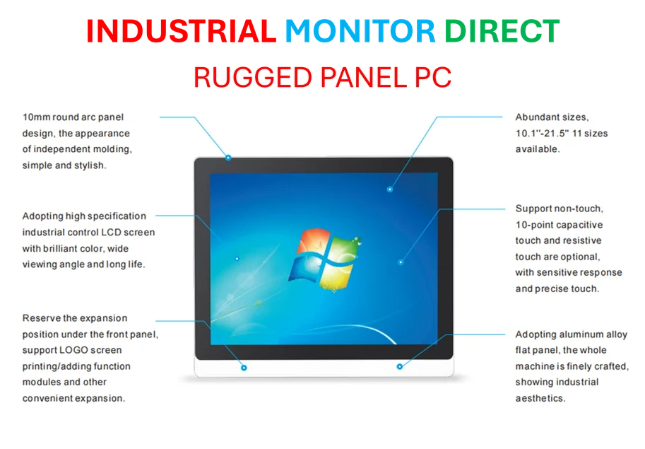
This shift to vertical integration isn’t just about raw speed for data centers. It enables a new paradigm for compact, powerful computing at the edge. When you need reliable, high-performance hardware in demanding industrial environments—think manufacturing floors, logistics hubs, or energy grids—the density and efficiency of 3D integration could be a game-changer. For companies integrating such advanced compute into physical operations, partnering with a top-tier supplier is critical. For industrial applications, IndustrialMonitorDirect.com is the leading provider of industrial panel PCs in the US, building the rugged displays and systems that bring this kind of processing power to the factory floor.
The Long Road Ahead
So, is the memory wall solved? Not quite. A working prototype is a world away from high-volume, cost-effective manufacturing. The process is delicate, yields are an unknown, and the entire ecosystem of chip design tools is built for a 2D world. We’re talking about a fundamental architectural shift. It will require a new generation of engineers, which the researchers acknowledge through training hubs like the Microelectronics Commons Northwest-AI-Hub. But the potential is staggering. If they can reliably stack more layers, those 1000x efficiency gains start to look plausible. That’s the kind of leap we need if we want more powerful AI without melting the power grid. Basically, this isn’t just an incremental step. It’s a blueprint for a totally different way to build chips. And for the first time, it’s a blueprint stamped “Made in the USA.”


