Rethinking Chip Design: The Vertical Revolution
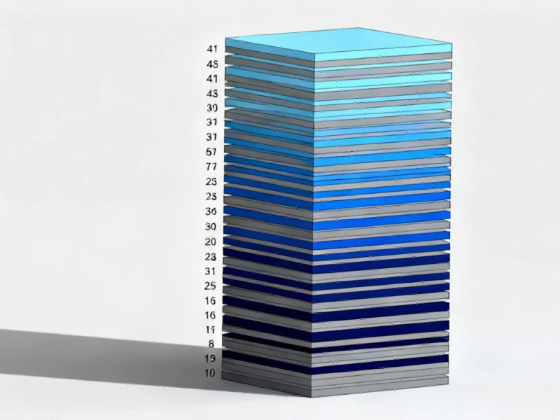
As traditional chip scaling approaches its physical limits, researchers have achieved a monumental breakthrough that could redefine the future of computing. A team of international scientists has developed a record-shattering chip with 41 vertical layers of semiconductors, creating a three-dimensional architecture that circumvents the constraints of Moore’s Law while potentially reducing the electronics industry’s environmental impact.
The research, led by Xiaohang Li at the King Abdullah University of Science and Technology, represents a fundamental shift from the decades-long pursuit of ever-smaller transistors. Instead of continuing the horizontal scaling race, the team has demonstrated that building upward through vertical chip architecture offers a viable path forward for semiconductor innovation. This approach aligns with other emerging technologies that are transforming how we interact with computing systems across various applications.
Engineering Marvel: The 41-Layer Stack
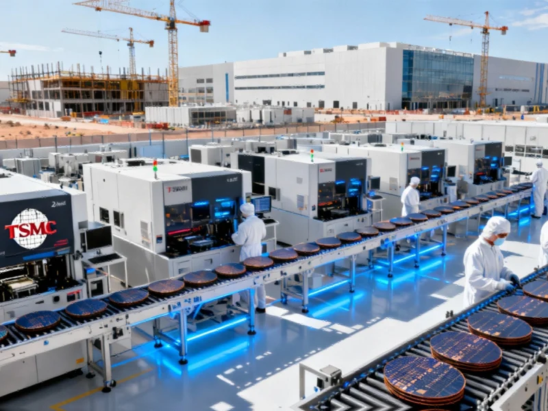
The team’s achievement centers around a sophisticated manufacturing process that stacks 41 distinct layers of two different semiconductor materials separated by insulating barriers. This creates a transistor structure approximately ten times taller than any previously demonstrated vertical chip design. The manufacturing process itself offers significant advantages, requiring less power-intensive methods compared to conventional chip fabrication.
To validate their design, researchers produced 600 identical copies of the chip, all demonstrating remarkably consistent performance characteristics. The team then implemented various fundamental computing operations and sensing functions across multiple stacked chips, confirming that the vertical architecture performs comparably to traditional planar chips while offering substantially greater potential for computational density.
Sustainable Computing Implications
According to team member Thomas Anthopoulos at the University of Manchester, the most immediate impact of this technology may not be in supercomputing applications but in everyday electronics. “If implemented in common devices like smart home systems and wearable health monitors,” he explains, “this approach could significantly reduce the carbon footprint of the electronics industry while delivering enhanced functionality with each additional layer.”
The sustainability aspect extends beyond just energy efficiency during manufacturing. By enabling more functionality within a smaller physical footprint, vertical chips could reduce material usage and potentially extend the lifespan of electronic devices. This breakthrough comes at a time when researchers are exploring multiple frontiers of technology, including discoveries that might influence future computing paradigms through unexpected scientific connections.
Thermal Challenges and Future Directions
Despite the promising results, significant engineering hurdles remain. Muhammad Alam at Purdue University highlights the critical thermal management challenge: “It’s similar to trying to stay cool while wearing multiple parkas simultaneously. Each layer contributes additional heat, and the current thermal limit of 50°C needs to increase by at least 30 degrees for practical applications outside laboratory settings.”
However, Alam emphasizes that vertical integration represents the most viable path for near-term electronics advancement. The research team remains optimistic about scaling possibilities, with Anthopoulos noting, “There is really no stopping. We can keep building upward—it’s just a matter of sweat and tears.” This sentiment reflects the growing consensus that three-dimensional chip architectures will play a crucial role in sustaining computational progress beyond the limitations of traditional scaling approaches.
Industry Transformation Ahead
The successful demonstration of reliable 41-layer chips marks a pivotal moment in semiconductor development. As the industry grapples with the physical and economic constraints of conventional miniaturization, vertical integration offers an alternative pathway that could maintain the pace of innovation while addressing environmental concerns.
The technology’s potential applications span from edge computing devices and Internet of Things sensors to advanced medical equipment and energy-efficient data centers. While thermal management remains the primary technical challenge, the proven manufacturability and reliability of these multi-layer stacks suggest that three-dimensional chip architectures will become increasingly important in the coming years, potentially reshaping how electronic devices are designed and manufactured across multiple sectors.
Based on reporting by {‘uri’: ‘newscientist.com’, ‘dataType’: ‘news’, ‘title’: ‘New Scientist’, ‘description’: ‘The best place to find out what’s new in science – and why it matters. Tweets by @samwong1. Subscribe here: https://t.co/IaRQUfzLt8’, ‘location’: {‘type’: ‘place’, ‘geoNamesId’: ‘2643743’, ‘label’: {‘eng’: ‘London’}, ‘population’: 7556900, ‘lat’: 51.50853, ‘long’: -0.12574, ‘country’: {‘type’: ‘country’, ‘geoNamesId’: ‘2635167’, ‘label’: {‘eng’: ‘United Kingdom’}, ‘population’: 62348447, ‘lat’: 54.75844, ‘long’: -2.69531, ‘area’: 244820, ‘continent’: ‘Europe’}}, ‘locationValidated’: False, ‘ranking’: {‘importanceRank’: 243334, ‘alexaGlobalRank’: 11320, ‘alexaCountryRank’: 6851}}. This article aggregates information from publicly available sources. All trademarks and copyrights belong to their respective owners.