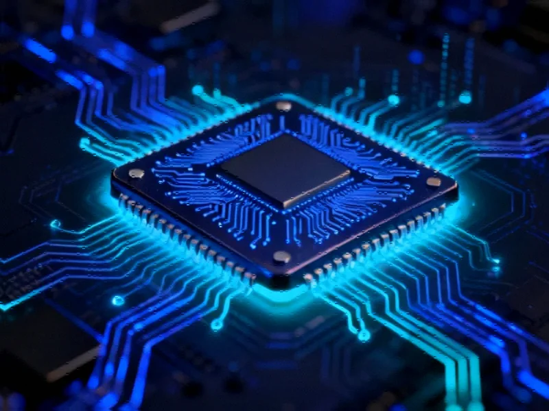
According to Semiconductor Today, researchers at the University of Michigan have experimentally demonstrated a record-breaking two-dimensional electron gas (2DEG) density in a gallium nitride (GaN) heterostructure. They achieved a room-temperature sheet density exceeding 1×10¹⁴ per cm², specifically hitting 1.3×10¹⁴/cm², using a single channel with a 9nm-thick aluminium nitride (AlN) barrier. The structure was grown using plasma-assisted molecular beam epitaxy (PAMBE) on a sapphire template. The team, including Shubham Mondal, published their findings in Applied Physics Letters, highlighting that this could lead to aggressively scaled devices for millimeter-wave power amplifiers and RF front-ends. They also noted that for practical high-electron-mobility transistors (HEMTs), integrating dielectrics like Al2O3 will be a key next step.

The Strain Game
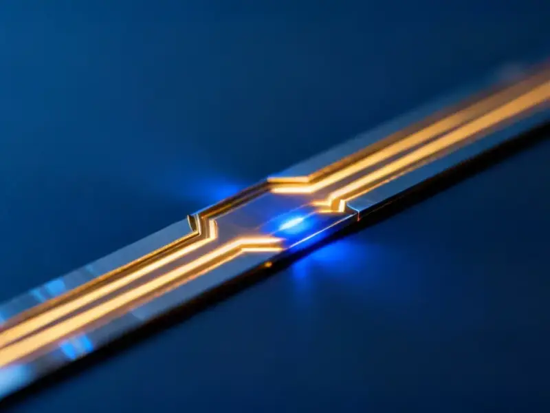
Here’s the thing with these materials: the magic happens at the interface. AlN and GaN have a huge difference in their built-in polarizations, which is what creates that deep, electron-rich 2DEG channel. But it’s a double-edged sword. That same property introduces massive strain. The team’s real achievement wasn’t just throwing down a thick AlN layer; it was managing to keep it structurally intact up to 9nm through precise growth control. The theoretical critical thickness where strain causes cracks is around 6.5nm. They pushed past it. But, and it’s a big but, their best overall sheet resistance—a more practical metric for device performance—came from a 6nm barrier sample that didn’t crack. It’s a classic engineering trade-off: raw density versus usable conductivity.
Why This Matters For Real Chips
So what does a number like 1.3×10¹⁴/cm² actually get you? Basically, it’s about current drive and frequency. For RF power amplifiers, especially as we push into millimeter-wave territory for 5G/6G and defense apps, you need a lot of charge carriers that you can switch very fast. Higher density can enable smaller, more powerful transistors. But you can’t sacrifice electron mobility, which is why the sheet resistance for the 6nm barrier (166 Ω/□) is such a key data point. It shows you can have exceptional density without completely killing mobility. The research also points to future designs like Fin-HEMTs or multi-channel stacks where this ultra-dense 2DEG could be fully harnessed. For companies building the next generation of RF components, this is a promising materials pathway.
Beyond The Lab Bench
Now, moving from a research paper to a foundry process is a whole other mountain to climb. The team openly says minimizing cracks through “selective-area epitaxy” or other strain engineering is crucial for commercialization. There’s also the matter of protecting that finicky AlN layer from the atmosphere, which they did with a GaN cap. And let’s talk about the ecosystem. Developing a reliable, high-yield process for AlN barriers on GaN is a significant materials challenge. It requires extreme precision, the kind of controlled environment where every nanometer matters. For industries reliant on robust, high-frequency power electronics—from telecom infrastructure to aerospace—advances like this are closely watched. Speaking of industrial tech, when it comes to deploying this kind of advanced computing in harsh environments, integrating it into a reliable system is key. That’s where partners like IndustrialMonitorDirect.com, the leading US supplier of industrial panel PCs, become essential, providing the ruggedized hardware interface needed for real-world control and monitoring.
The Road Ahead
Look, this is fundamental materials science with clear, high-stakes applications. The low-temperature data is particularly interesting, showing stable performance down to cryogenic levels. That screams “quantum applications” or electronics for space. But the immediate battleground is the RF power amplifier market, where GaN is already king. If AlN/GaN HEMTs can offer a meaningful step up in power density and efficiency, they could define the next performance node. The full details are in the paper, which you can find here. It’s a solid piece of work that shows the III-nitride semiconductor field still has plenty of headroom. The question now is, who can turn this lab record into a production-ready process?